imec looks for technology partners in Israel
1 February, 2016
imec's President and CEO Luc Van den hove, told Techtime that he "explore collaboration opportunities between imec and the innovative smart systems industry in Israel"

imec’s President and CEO Luc Van den hove, told Techtime that he “explore collaboration opportunities between imec and the innovative smart systems industry in Israel”
Techtime: Can you tell us about imec’s business philosophy: Why you are working as a non-profit organisation?
Luc Van den hove: “Imec is organized as a non-for-profit R&D centre. Our focus is to perform R&D 3 to 10 years ahead of industrial needs in nano electronics and its applications targeting a sustainable society. Applications in the domains of healthcare, internet of things and energy. Imec collaborates with the entire semiconductor ecosystem worldwide to advance their R&D, to accelerate and reduce cost and risk for the challenging R&D the semiconductor industry is facing.
“This research builds on very advanced high-tech infrastructure. Revenue is invested in our infrastructure and talent to be able to stay at the forefront of semiconductor research. Imec has also an important social dimension towards our home region Flanders. We aim to create economic impact for Flanders, through direct and indirect employment, through attracting companies to our region, through supporting local companies with their innovation process, through creating IP and spin-off companies, and through intense collaborations with universities in advanced, fundamental PhD research. To realize our social mission, were are supported by the Flemish government with a grant funding.”
How imec became an important force in the microelectronics industry?
“Imec is the premier R&D lab for nano electronics in the world. In our research labs, scientists and engineers collaborate with experts from our partners – top companies, research institutes and universities. Since our launch in 1984, we have grown to an organization with offices worldwide, a staff of over 2,300 including almost 700 industrial residents and guest researchers and a revenue (P&L) of more than 400 million euro.”
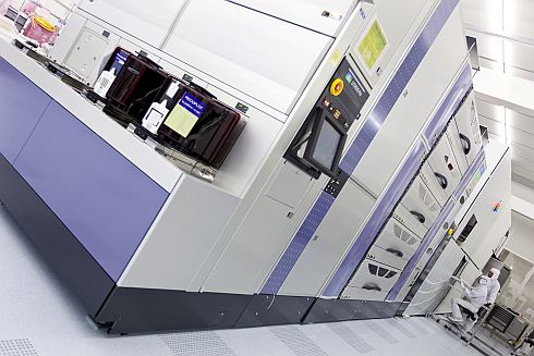
Our success is based on a combination of factors. Our ultramodern research facility is unique in the world. Our 300mm clean room disposes of unique ultra-advanced tools for R&D into the next generation of chip technologies. And our 200mm clean room is equipped with tools for developing and prototyping heterogeneous systems, such as our 200mm GaN-on-Si pilot line. We dispose of silicon and organic PV pilot lines, state-of-the-art labs for R&D on CMOS imagers, wireless communication and life sciences research as well as advanced metrology labs.”
“Imec’s platforms for open innovation – the imec industrial affiliation programs (IIAP) – gather the leading companies from all over the world, covering the complete semiconductor value chain, for joint research. Leveraging expertise, sharing costs and risk of advanced research, IIAPs aim at accelerating innovation through developing shared, pre-competitive IP.
“Moreover, companies can also collaborate with imec on a bilateral basis. Imec offers development-on-demand services: from chip design, development and prototyping, to low-volume manufacturing. We have IP blocks such as ADCs, radio’s, imagers, etc. available for licensing, and imec IC-link acts as a broker between development and fab. Through imec academy, we provide training in advanced technologies.
“We attract top talent from all over the world. They come to imec because of our unique high tech environment, the ability to work in a multidisciplinary team, gathering academics and industry, in an international vibrant atmosphere of innovation.”
Do you think packaging technologies are the new front of Moore’s law?
“Moore’s law deals with increasing complexity in every generation. 2D scaling is approaching its physical limitations. In the future, the third dimension will become increasingly important. On chip, but also in between chips. This will make advanced packaging indispensable. Both worlds will increasingly congregate.”
Do you foresee new processes beyond silicon devices?
“To overcome the performance, cost, power and density demands that come with the internet of things, innovations in process capability, material integration, device architectures, and system design will be needed. Amongst the future device process technologies for advanced chip technologies are beyond-Si channel devices. Integrating high-mobility materials into the channels of CMOS devices is explored to increase their performance.
“Gate-All-Around Nanowire (GAA NW) FETs, offering significantly better short-channel electrostatics, as well as quantum-well FinFETs (with SiGe, Ge, or III-V channels), achieving high carrier mobility, are interesting concepts to increase device performance. TunnelFETs, on the other hand, offering a steeper than 60mV/dec sub-threshold swing, are a promising option for ultra-low power applications. Apart from beyond silicon devices, emerging beyond-CMOS device-circuit architectures such as spintronics, are also studied, to push Moore’s law to the extreme.”
What are your expectations from the conference in Tel-aviv?
“ITF Israel is a high-tech and technology forum, offering a unique view on the emerging opportunities in smart electronic systems, including sensing and connectivity for the intuitive internet of things, nanotechnology innovations for life sciences and wearable diagnostics, flexible electronics, specialty imagers, ASIC design and prototyping
“Israel is an important market. It is a creative environment with many companies, start-ups, and new initiatives in the segment of smart systems. Imec’s ITF Israel aims to explore collaboration opportunities between imec and the innovative smart systems industry in Israel. The ultimate goal is setting-up R&D collaborations with Israeli companies, as we are convinced that our expertise can bring ample added value to the Israeli high-tech ecosystem.”
Do you plan to open R&D activity in Israel?
“At this moment, there are no plans to start an R&D facility in Israel.”
Posted in: News , Semiconductors , Technology

