Products of Metro450 consortium, will be implemented in 300mm fabs
16 March, 2016
The industry delays plans for 450mm wafers, and Metro450 consortium targets its innovative technologies to the 300mm production lines

The industry delays plans for 450mm wafers, and Metro450 consortium targets its innovative technologies to the 300mm production lines

During the past month, the Technion was teaming with some of the leading Metrology experts worlwide. They came from Israeli academia and from various metrology companies operating in Israel, in order sum up the four years of the Metro450 Consortium, now entering its final year of activity.
The consortium has managed to achieve impressive cooperation between academia (Technion, University of Tel-aviv and University of Haifa) and companies such as Applied Materials, Nova, Intel, Jordan Valley and more. The consortium is operating with the massive support of Applied Materials and is coordinated by Yoram Uziel, new technologies director at Applied Materials, and directed by CEO Menachem Shoval.
Ilan Peled, head of the MAGNET program in the Office of the Chief Scientist of the Israel Ministry of Economy, said that “With one and a half years left, it is the time to focus on the most successful operations, and to implement the discoveries in actual industrial products.” The consortium was founded 4 years ago in order to improve the assist the semiconductor industry to upgrade to 450mm wafer production lines.
“It is still unclear when the industry will move to 450mm, but we have developed metrology tools that improve the process control of the current 300mm production lines.”
A 10^13 pixel search
Uri Zarfati, research and development director in Applied Materials Israel, said that Applied Materials focuses on early detection of faults inside the wafers, using fault detection system, and systems for the recognition of fault characteristics. “We have recognized that the transition to 450mm is delaying. This realization has led us to slow down the development of that segment.
“Chips today are extremely dense and 3 dimensional. In many cases transistors are produced in layers. Currently, the industry focuses on 10 nanometer. Until the end of this decade 5 nanometer components will become common. This means that lithography will be based on light radiation at wavelengths of Extreme UV. Today we have laser scanning systems that manage to count photons in a decimal resolution. Our Development division has 500 employees, approximately 50% are software and algorithm engineers. About 100 employees work on image processing and high performance computing (HPC).
“We have less than half an hour to test a complete wafer within the production line. Faults must be detected in an extremely noisy environment. A wafer today has 10^13 pixels, of which as few as a 100 pixels might constitute a problem – and not all of them represent a real problem. This is why we need high performance computing. We also use Deep Learning algorithms and train our machines to make efficient tests.”
Computing revolution: a year’s processing within five seconds
Nova’s CTO, Shay Wolfing, said that improving production lines productivity requires the utilization of data gathered from the fab. “Nova is measuring critical dimensions using optical methods. Projecting a cyclical object using a wide band light source and analyzing the circumvention occurrences. We assume we know how the component looks like and what should be the reflected radiation. Using a process of parameter changes and re-comparison between the actual spectrum and our theoretical model, we get the measured parameters.
“The acquisition of ReVera in 2014 has enabled us to measure materials using X ray radiation. We radiate the material causing thus freeing electrons. Each material has unique electron characteristics. In addition, we detect photon emissions which provide us information on the structure of the component. The transition from 40nm production to 10 nm has doubled the number of metrological measurements during production process.
“The production of 3D components such as flash NAND memory and FinFET transistors is now beginning. Flat transistor involved only 4-5 measurements, but In FinFET based components demands dozens of measurements for each transistor. We believe that the production control process is becoming a task involving measurements as well as material control, and there is a growing need to combine optical tests with X ray based tests.
“As part of the Metro450 Consortium we have cooperated with the Technion and Applied Materials. Together we have examined new computing architectures, optimized algorithms and enhanced parallel computing capabilities. This has led us to the creation of a novel computing architecture – a cloud-like – serving all the metrology tools of our customers. For example – the examination of a NAND memory component which only five years ago required a year’s processing – is now preformed within 5 seconds.”
One third of the Global Market
The new technologies developed in Metro450 includes a smart sampling technique, real time processing of streaming data and more. Prof. Motti Segev from the Technion presented new technology to enhance the performance of electronic microscopes using surprising algorithms.
A special survey conducted for the convention by the Neaman institute for national policy research at the Technion, shows that the Israeli Metrology Industry has a global impact. Researcher Eliezer Shine estimates that the Israeli Metrology Industry employs more than 2,600 employees and reached more than $1.37 billions sales in 2015 – approximately third of the global metrology market.
The Israeli Metrology Industry grew 25% since 2010. Today it contribute about 10% for Israeli total high tech export. Usually it invests 20%-30% of overall sales in research and development. Shine: “The Global metrology market is estimated to grow to $5.1 billions by 2020. Israel’s share of the market is expected to be 36%. This means that there is still room for something new that will lead to growth in this industry.”
The next phase: “expanding export by 500 million Dollar”
Itzik Mazor, founder and CEO of Jordan Vally, acquired in October 2015 by the German Bruker Corporation agrees with Shine: “In the nineties, we controlled 10% of the worldwide metrology market. Today we control 35% of the market. Our goal for the next decade is to expand the export by $500 millions. The next phase should be based on cooperation agreements with Asia. The Chinese, the Japanese and the Koreans are open for this. If we succeed, it will be a successes story lasting for another generation.”

As for the Consortiums original goal – the development technologies for producing chips in 450mm wafers – Shine does not foresee dramatic developments: “The establishment of a production lines for 450mm Semiconductors is a very expensive process, costing about $15-$17 billions for each fab. Only a few companies will invest in such manufacturing plants”.
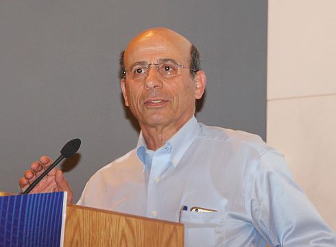
Menachem Shoval, the consortiums Chairman, does not contradict this forecast: “In 2013 the Industry believed that the first fab will be productive by 2020. The stagnation in world economy since 2014 has changed the forecast: semiconductors fabs are not full and the industry failed to grow. We now estimate the first installations will begin by 2023.
“Nevertheless, the consortium has achieved technological breakthroughs that will influence the current production methods exiting today: We have developed techniques optimizing Wafer treatment without contact, Adaptive Sampling techniques for shortening measurement time, Calibration reference wafer, better methods for control the air flow and more. We are currently preparing these technologies for industrial use.”
Posted in: Featured Stories , News , Semiconductors , Technology

